


Microfabrication process
CVD, PVD, Etching
CVD
CVD(Chemical Vapor Deposition) is a film forming method performed by chemical reactions.
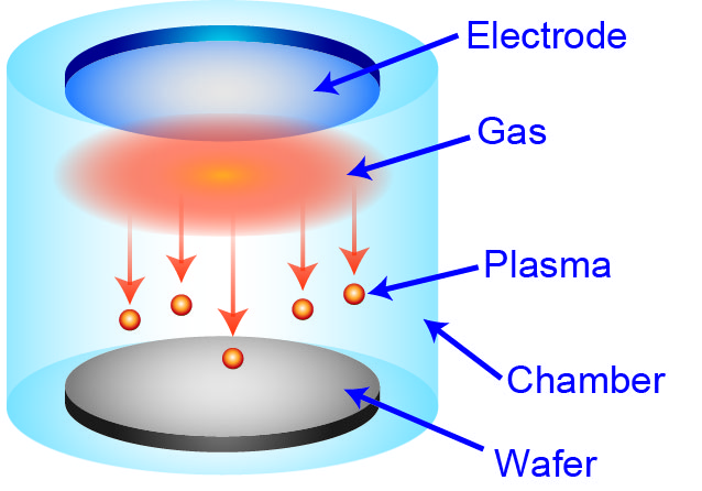
Plasma is generated by applying RF to the gas enclosed in the chamber. When generated plasma reaches the wafer, chemical reactions occurs on the wafer surface. The combination of wafer and gas determines the type of film to be deposited. For example, when N2(nitrogen) gas and Si wafer are used, SiN(silicon nitride) is deposited.
PVD
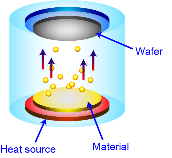
PVD(Physical Vapor Deposition) is a film forming method by depositing metal molecules.
Evaporation method : Heat the metallic material and evaporate it.
Ion plating method : Form a film with higher adhesion than Evaporation method. Evaporated metal particles are charged by plasma.
Sputtering method : Hit plasma against metal surface and metal particles that jumped out are deposited on the wafer.
Etching
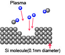
Etching is a method of processing wafers with chemicals or plasma. With plasma, micro scale etching is possible. Etching improves various technologies (miniaturization of recording devices such as HDD, creation of MEMS, and so on).
Please feel free to contact us if you have any problems with plasma.